Questions? 800-523-5874 | [email protected]
- TEM Grids
- Prepmaster™ Specimen Preparation Robot
- TEM Window Grids
- Omniprobe Nanomanipulation Systems
- K-kit Wet "Liquid" TEM Kit
- Specimen Mounts
- SEM Specimen Holders
- Index and Finder SEM Grids
- SEM for Forensics
- SEM Sample Preparation Station Materials
- Cryogenic Personal Protection Equipment
- Cryo Dewars & Flasks
- Cryo-EM Grids & Grid Storage
- Cryogenic Vials & Racks
- Cryo-EM Vitrification Supplies
- Prepmaster™ Specimen Preparation Robot
- Laboratory Microwave Ovens
- LYNX II Automated Tissue Processor
- EMS Poly III
- Microtomes
- Tissue Slicers
- Heaters & Chillers
- SEM Cooling Stage
- Glow Discharge Systems
- Sputter Coaters & Carbon Coaters
- Stages
- Freeze Dryers
- Critical Point Dryers
- Cryo-SEM Preparation System
- Specimen Transfer Systems
- Decontaminators
- Desiccators
- Centrifuges
- Dry Baths
- Stirrers, Hot Plates
- Vortexers & Magnetic Mixers
- Rotators & Rockers
- Ovens & Incubators
- Vibration Isolation
- Air Sampling
- Vacuum Pumps
EMS Technical Data Sheets

Cleaving Copper C4 Bumps with LatticeAx
EMS Catalog #7641
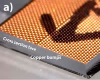
Copper Bumps After Cleave
This sample was prepared by using a Multi-tool workflow.
The preparation yielded a high-quality cross section ready for SEM imaging.
 |
 |
|
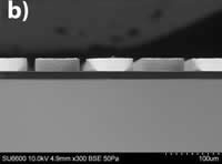
| After Step 1: SEM | SEM image showing direction on ion mill poilish |
The solder bumps were prepared for the SEM in a two-step process.
In Step 1, the LatticeAx™ cleaver was used to cleanly cross-section close to and parallel to a specific row of copper bumps. The copper bumps had a diameter of 85-µm and were cleaved 30-µm from the center of a bump.
The time to cleave was 5 minutes.
 |
 |
|
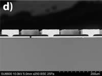
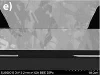
| After Step 2: SEM after cleave and polish | SEM image through center of bump |
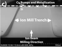
In Step 2, a broad, argon, ion-beam instrument, the Hitachi IM4000, was used to prepare the final imaging surface.
The sample was mounted topside down on a sample block to perform backside milling. Backside milling was used to prevent artifacts of ion beam milling that can occur as a result of sample topography. By cleaving close to the center of the copper bumps, the time on the ion mill was minimized. No further preparation was performed.
Additional Technical Data Sheets
LatticeAx™ FAQ Technical Data SheetLatticeAx™ Technical NoteTechnical Data Sheet
Product Information
The LatticeAx™