Questions? 800-523-5874 | [email protected]
- TEM Grids
- Prepmaster™ Specimen Preparation Robot
- TEM Window Grids
- Omniprobe Nanomanipulation Systems
- K-kit Wet "Liquid" TEM Kit
- Specimen Mounts
- SEM Specimen Holders
- Index and Finder SEM Grids
- SEM for Forensics
- SEM Sample Preparation Station Materials
- Cryogenic Personal Protection Equipment
- Cryo Dewars & Flasks
- Cryo-EM Grids & Grid Storage
- Cryogenic Vials & Racks
- Cryo-EM Vitrification Supplies
- Prepmaster™ Specimen Preparation Robot
- Laboratory Microwave Ovens
- LYNX II Automated Tissue Processor
- EMS Poly III
- Microtomes
- Tissue Slicers
- Heaters & Chillers
- SEM Cooling Stage
- Glow Discharge Systems
- Sputter Coaters & Carbon Coaters
- Stages
- Freeze Dryers
- Critical Point Dryers
- Cryo-SEM Preparation System
- Specimen Transfer Systems
- Decontaminators
- Desiccators
- Centrifuges
- Dry Baths
- Stirrers, Hot Plates
- Vortexers & Magnetic Mixers
- Rotators & Rockers
- Ovens & Incubators
- Vibration Isolation
- Air Sampling
- Vacuum Pumps
EMS Technical Data Sheets

LatticeAx™ E-beam Lithography
EMS Catalog #7641
Successful Cleaving of Delicate Nanostructures Fabricated Using E-Beam Lithography
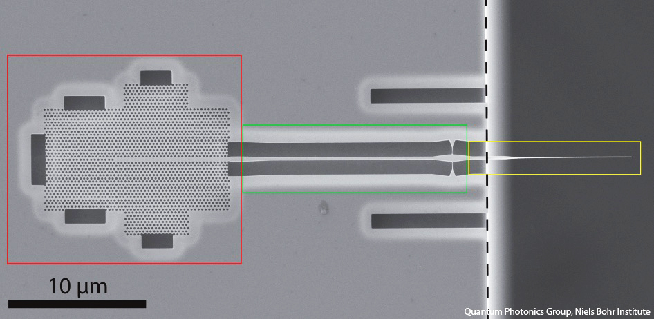 Scanning Electron Microscope image shows one of the nanostructures after cleaving with the LatticeAx 420. Courtesy of the Quantum Photonics Group, Niels Bohr Institute, University of Copenhagen.
Scientists in the Quantum Photonics Group at the Niels Bohr Institute of the University of Copenhagen are developing new technologies for photonic and quantum-information applications used the LatticeAx to alleviate one of their biggest sample preparation challenges: precise cleaves on small samples without damaging delicate fabricated nanostructures.
As part of this research, the team has developed processes whereby they fabricate suspended photonic crystals and other nanostructures using GaAs. The nanostructures themselves are between 160 and 180 nm thick. To perform experiments on these structures, the team needed to be able to cleave small samples without damaging the small and delicate devices that they had fabricated. And they absolutely required a method that minimized sample handling to further reduce the potential for damage to the nanostructures.
Contact us for the use case to learn more about how a successful process was developed to cleave these delicate fabricated samples.
"... we were able to spend less time preparing samples, with less wasted material in each run."
-Tommaso Pregnolato, Ph.D. Fellow
Product Information
The LatticeAx™